

Introduction:
The semiconductor complex laboratory is responsible for designing and developing Very Large Scale Integration (VLSI) circuits to meet the demand of Application Specific Integrated Circuit (ASIC), Opto-electronic, and Micro-Electro-Mechanical System (MEMS) devices. It fulfills the requirements of the Department of Space (DOS), Indian Space Research Organization (ISRO), Defense Research Development Organization (DRDO), Indian railways, and other strategic wings of the Govt. of India. Its operation includes wafer fabrications, assemblies, packaging, testing, and quality assurance.
It has two wafer fab lines (i) 8” CMOS (Complementary Metal Oxide Semiconductor) in 180 nm CMOS Technology and (ii) 6” fab lines with both CMOS and MEMS technology. It produces high reliable electronic board, Radio Sonde system, and integration of the various sub-system.
Details Description:
The industrial visit takes place on 28 Sep 2022 at 10:30 a.m. under the supervision of Dr. Sovan Mohanty and scientist from SCL, Chandigarh. Initial presentation includes the detail mission and objective of the laboratory, to create a self reliant India in the field of micro-electronics and communication technology. It includes Space, Optoelectronics, Defense applications, etc. It is followed by visit to the fab lab having class-1, class-10, and class-100 clean room set up. Students are instructed and demonstrated various practical aspects of Doping, Oxidation, Etching, Photo-lithographic, metallization, and packaging of processor chips. Students queried about the details of the fabrication process.
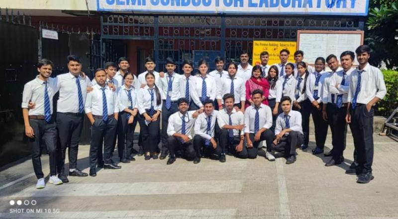
Travel Details:
This industrial visit has a team of two faculties and 29 students combined from the final year and third year of ECE. The journey started on 27 Sep 2022 at 06:30 A. M. by bus from Bareilly to Chandigarh. The team reached Chandigarh at around 09:30 P. M. and stayed in a Hotel. On 28 Sep 2022 team visited the fab laboratory and stayed there up to 02:00 P.M. After lunch team visited Rock garden, and by 06:00 P. M., they left Chandigarh for Bareilly.
Conclusion:
This visit provided a strong relationship between Industry and Academia by creating technical awareness about cutting-edge technology among students. This visit will help create a strong R & D base in the country, especially in the field of Microelectronics and Semiconductor manufacturing.